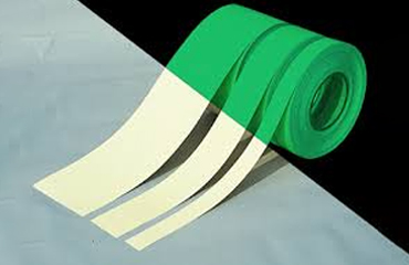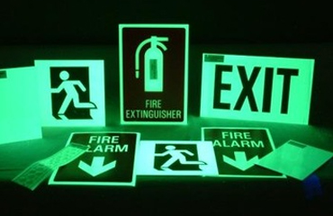
Non-Toxic Photoluminescent Material
Be that as it may, their applications are constrained on the grounds that it is difficult to create QD thin films, they utilize dangerous starting materials like cadmium and lead, and orchestrating them is costly.
Some photoluminescent zero-dimensional (0D) materials (i.e. materials in which electrons are confined to a few nanometers and can be excited to produce light) have been tested, but they still relied heavily on lead.
Thus, scientists at Tokyo Tech, led by Prof. Hideo Hosono, designed a novel photoluminescent lead-free 0D material and analyzed it to gain insight on the nature of photoluminescent materials. The material called Cs3Cu2I5, has a crystalline structure.
Prof Hosono said, “The thin film exhibited good stability under ambient conditions, that is, no noticeable degradation in photoluminescent quantum yield (PLQY) over two months.”
The group went above and beyond and exhibited two applications utilizing this material. The first was a white luminescent film, manufactured by blending the blue-radiating material with a yellow phosphor at a particular proportion to create white light.
As appeared in Figure, films that emanate light of different hues could be set up by fluctuating the ratio of the fixings utilized. The second application was a blue LED, which lamentably showed poor electroluminescence (EL) performance. Be that as it may, this enabled the group to more readily comprehend the basic EL instruments, which will be valuable in future research.
Hosono said, “The exploration of low-dimensional compounds based on a Cu(I) halide proved to be a novel route obtain a Pb-free high-PLQY luminescent material. Such materials will hopefully see the light of day in future optical and nanotechnological applications.”